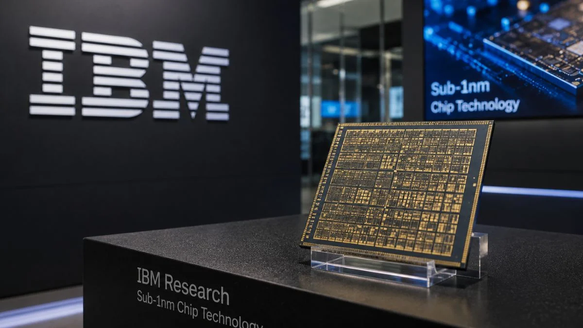
How IBM’s New Sub-1nm Chip Could Redefine AI Hardware
In Focus
- IBM’s sub-1 nanometer chip can hold close to 100 billion transistors
- IBM used the Nanostack architecture to build the new chip
- The chip can perform about 50% more tasks compared to the previous generation
IBM has introduced a technology that can produce sub-1 nanometer chips. The technology represents a major breakthrough as tech companies compete to develop powerful chips to handle demanding AI workloads. News about IBM’s chip technology comes at a time when chipmakers globally are exploring ways to pack more computing power into much smaller spaces.
This approach is mostly associated with Moore’s Law, which describes the trend of packing more transistors onto a chip. Engineers do this by shrinking transistors, which are the tiny switches responsible for computations, to smaller sizes.
Why Does IBM’s Sub-1 Nanometer Chip Matter?
IBM’s next-gen chip technology breakthrough matters because it could be instrumental in fast-tracking chip innovation. Currently, chipmakers struggle to shrink transistors. IBM’s technology uses a three-dimensional transistor architecture known as Nanostack.
The architecture stacks transistors vertically to enhance density while improving performance and energy efficiency. According to the company, Nanostack is the industry’s first nanosheet-based design that can support chip production below the 1-nanometre threshold.
“It’s not just an incremental step. It’s a meaningful leap forward,” IBM’s Research Director, Jay Gambetta said as cited by the MIT Technology Review.
IBM said its sub-1 nanometer semiconductor can hold close to 100 billion transistors on a fingernail-sized chip. This represents a significant leap in transistor density. If achieved at scale, the technology could double the density of IBM’s 2 nanometer chip prototype unveiled in 2021.
How Efficient is IBM’s Sub-1 Nanometer Chip?
IBM reports show that chips developed using nanostacking technology can handle higher workloads and are more energy efficient. The company said the new chips can perform about 50% more tasks compared to those built using the state-of-the-art architecture. They also consume up to 70% less energy than the previous ones.
IBM’s, which unveiled Power 11 AI chips last year, said the new chip architecture supports different materials across stacked transistor layers. This allows engineers the flexibility to optimize each layer independently for speed, power consumption, or energy efficiency, which boosts chip performance and efficiency.
Nanostacking technology paves the way for the production of more powerful processors for AI and cloud computing workloads. According to Gambetta, the technology will be used widely in data centers over the next decade as companies explore ways to improve energy efficiency.
What Next for IBM?
After unveiling the world’s first sub-1 nanometer chip, IBM plans to partner with semiconductor manufacturing firms to produce the sub-nanometer chips. The company expects chip designers to deploy the design across multiple chip types, including CPUs and GPUs.
“I expect to have many conversations with designers about how they can use this technology,” IBM’s VP for Global Semiconductor R&D, Huiming Bu, noted.